Cadence Stock Breakdown

Get smarter on investing, business, and personal finance in 5 minutes.
Stock Breakdown
Imagine you wanted to design a city to minimize traffic.
It wouldn’t be good enough to just draw up a paper blueprint — you’d want a full 3D simulation.
You’d then run rush-hour scenarios, accidents, weather events, construction shutdowns.
You’d stress-test every road before building anything.

Now imagine shrinking that entire city to the size of a quarter.
Then turn every:
1) road into a wire
2) every intersection into a transistor
3) every traffic jam into excess heat, power loss, or a lost signal.
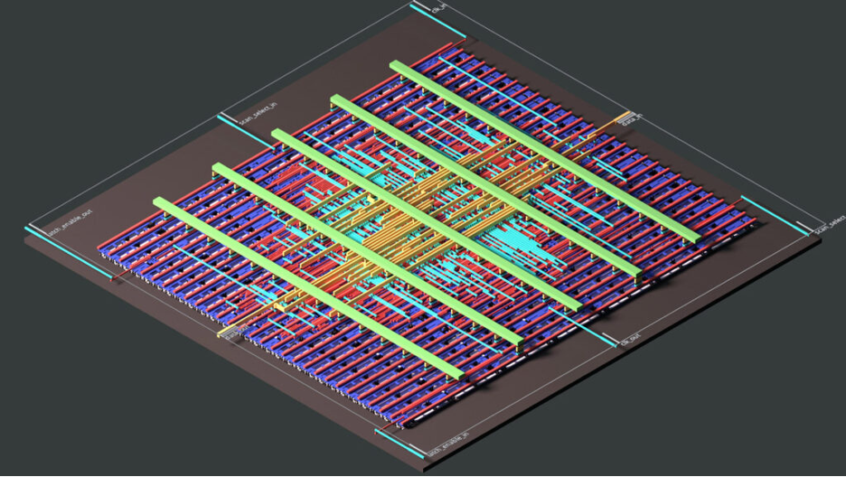
That’s essentially what modern chip design is.
Today’s advanced chips contain billions of “roads” and “intersections”, all operating at nanosecond speeds.
And you can’t fix problems after the chip is built. One mistake can cost hundreds of millions of dollars and months of lost time.
This is why chips aren’t designed by humans anymore — they’re designed by software.
And one of the largest companies building that software — the one quietly determining whether AI, data centers, cars, and smartphones actually work — is Cadence Design Systems.
What Cadence does
Modern chips contain billions of transistors.
Each bundle of transistors that specifies a particular operation is called a block.
Each block will specify a particular operation, like “add”, “multiple”, or “remember this”.
Engineers will use a hardware language that writes what various “blocks” are supposed to do.
A medium sized block can have anywhere from 10,000 to 1 million transistors.
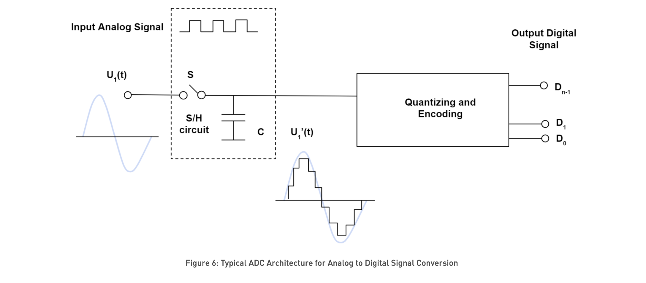
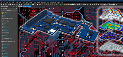
Instead of a human figuring out by hand how to arrange these transistors for each block, they rely on EDA tools.
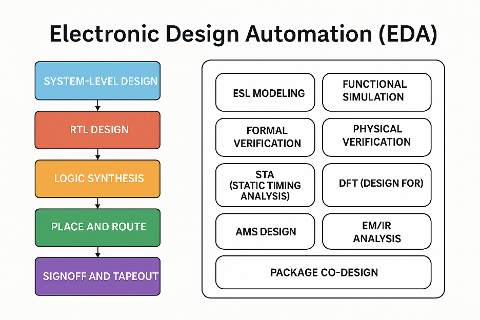
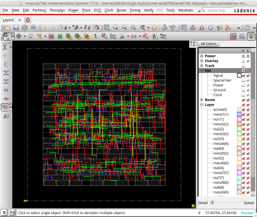
The EDA software decides where to layout the millions of transistors and route microscopic wires in between them.
The design needs to take into account factors like heat, speed, and potential signal loss.
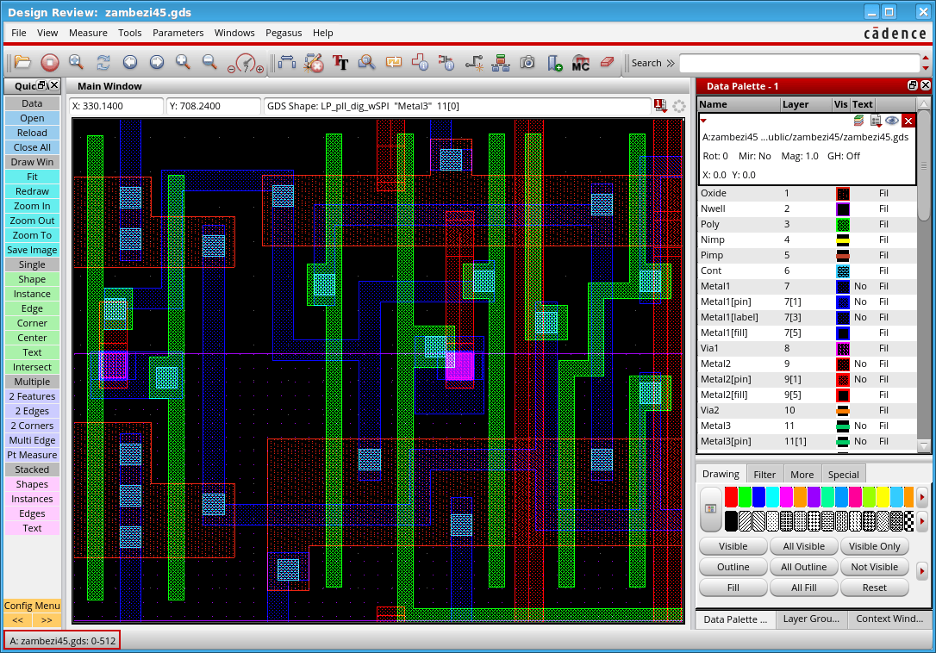
This step of taking the “abstract chip architecture” into a “physical layout” is a key aspect of EDA software.
This is just the beginning steps to turn a chip idea into a physical creation.
Getting the initial physical layout is like designing a gameplan that has never been run. Once you test it in the real world, you see all sorts of issues that need to be ironed out.
In the initial chip design the engineers were just figuring out what they ideally like the chip to do—they use tools like Cadence’s Genus Synthesis and Innovus Implementation system to do this.
Now not every part of the chip design can be automatically generated by software. These are the analog components like:
1) power delivery circuits—distribute stable voltage
2) clock generators—create timing signals
3) memory cells—store data
4) high-speed input/ output interfaces—move data inside and outside the chip
Because small variations can break the whole chip design, they are manually designed at the transistor level.
Engineers can use Cadence’s Virtuoso and Spectre tools to hand-craft and simulate these analog and custom blocks early in the process.
After that though they have to check that it actually does what is intended. This is where the next step comes in.
Chip Design Checking Process.
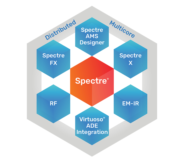
1) Simulation and verifications.
This is about whether the chip is behaving as the designer intended it to.
The question the engineer is answering here is: What happens if I run this?
Cadence’s Xcelium, Spectre, and Jasper Formal Verification tools help with this.
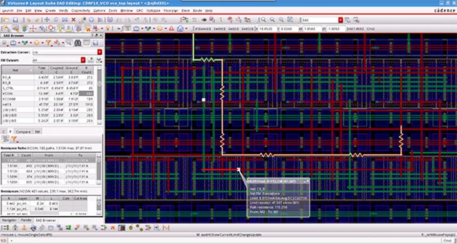
2) Timing, Power & Reliability (Signoff)
Even if a chip behaves correctly, it can still fail if signals arrive too late, power delivery collapses, or heat degrades performance. (More on this momentarily).
The question here is: Will this still work under worst-case real-world conditions?
Cadence’s Tempus and Voltus tools analyze signal timing, power spikes, voltage drop, and long-term reliability.
3) Manufacturability.
A chip can be logically correct and physically stable, but still impossible to build reliably at advanced nodes.
The question here is: Can a foundry actually manufacture this design at scale?
Cadence’s Pegasus and PVS tools verify that the layout follows strict manufacturing rules and matches the original design intent.
4) Packaging Validation.
A chip still has to communicate with the outside world and survive heat, power, and signal integrity challenges beyond the silicon itself.
The question here is: Does this chip still work once it’s packaged and put into a real system?
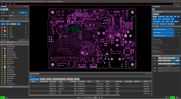
Cadence’s Allegro, Sigrity, and Clarity tools simulate packaging, circuit boards, and system-level physics.
Real World Simulation.
Key to understanding Cadence is to understand how often a theoretical design has errors.
Figuring out issues before the chip is actually produced is key though because the chip fabrication process can cost hundreds of millions of dollars and if there is an error in the chip design, the whole project needs to be scrapped.
This is where Cadence Design really adds value.
They have several simulation tools (mentioned above) that can test a chips design in real world conditions before they produce it.
Engineers will run these simulations repeatedly in order to uncover:
• Timing failures
This could be because wires are too long, transistors slow down when heated up, or multiple blocks compete for power. It is problematic because the chips then read wrong values, run slower, or totally fail.
• Power Spikes
This is caused by too many transistors turning on simultaneously or inadequate power delivery design. This can trigger shutdowns, corrupt data, and damage the chip.
• Single Interference
This is because the wires on a chip are too close and the electric current distorts a neighboring signal. This causes unpredictable bugs, can corrupt data, and can randomly fail.
Cadence’s stack of design tools helps with all of this.

Competitive Advantage.
Cadence’s advantage stems from three sources.
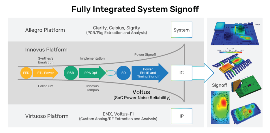
1) The first is that they have an entirely integrated tool set that designs and tests, not just the chip, but the system.
As we saw above, there is a Cadence tool that helps with every step of chip design and can pass off the chip design from one stage of the process to the next.
If you want to design the whole chip in one flow, Cadence is the best option.
2) They also are by far the strongest with analog.
This is also called “mixed signals” and is when there is a physical world aspect to the chip.
Most engineers are trained on Cadence’s Virtuoso, which is very hard to switch out of a workflow.
3) Cadence is also the leader with how a chip will actually behave once it is soldered onto a chip board and placed in a device.
They own Allegro, which is an industry leader for testing a chip on a circuit board, and Sigrity, which tests how well the signal works in the real world.
They also have the Celsius Thermal Solver which simulates nuances such as how airflow of a chip in a car can get impact how hot the chip gets.
4) They also have a leading hardware emulation tool—Palladium.
This is a real world supercomputer that transforms its internal pathways to mimic the prototype chip logic. This allows a chip designer to test the chip much faster than software emulation.
Once a tool becomes an industry standard, foundries like TSMC may require a chip designer do such testing using them to avoid a situation where they fabricate a chip with an error.

Future Growth Areas.
Cadence is looking to increase their advantages going forward with:
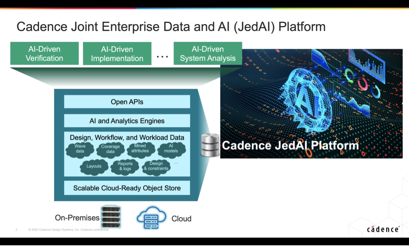
1) AI-Driven Design Tools. These tools like the JedAI platform use AI to find the best placement of transistors for a more efficient chip.
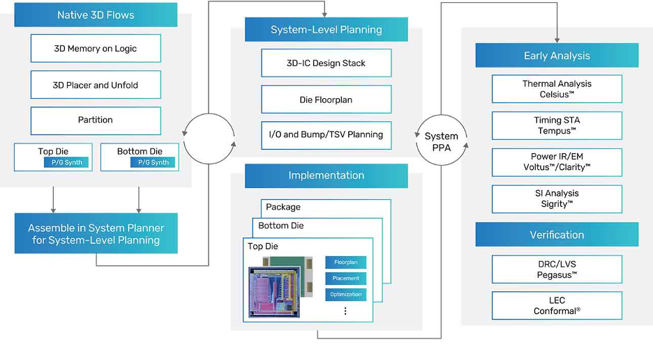
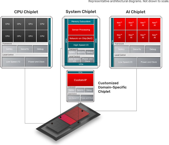
2) Chiplet Leadership. Chips are becoming too complex to build on a single piece of silicon, so the industry is moving to “Chiplets”. These are specialized piece of a chip designed to be packaged with other chiplets to make a “full chip”.
Cadence’s Integrity 3D-IC platform is currently the most complete tool for designing these 3D chip packages.
Key Risks… or Opportunity?
Chips are moving away from copper wire.
Instead of electricity running on tiny copper wires, semiconductor companies are trying to move a chip to transfer signal with light.
This is 100x faster.
This new area is creating a new breed of so called photonic design tools.
Cadence used to partner with the leader—Ansys—but competitor Synopsys bought them for a whopping $35 billion.
Candence made a couple acquisitions and is now trying to build their own in-house solution.
While it is unlikely that the new Synopsys/ Ansys displaces Cadence’s core design business, it could cap their growth, especially if they become the industry standard.

But What is the Upside?
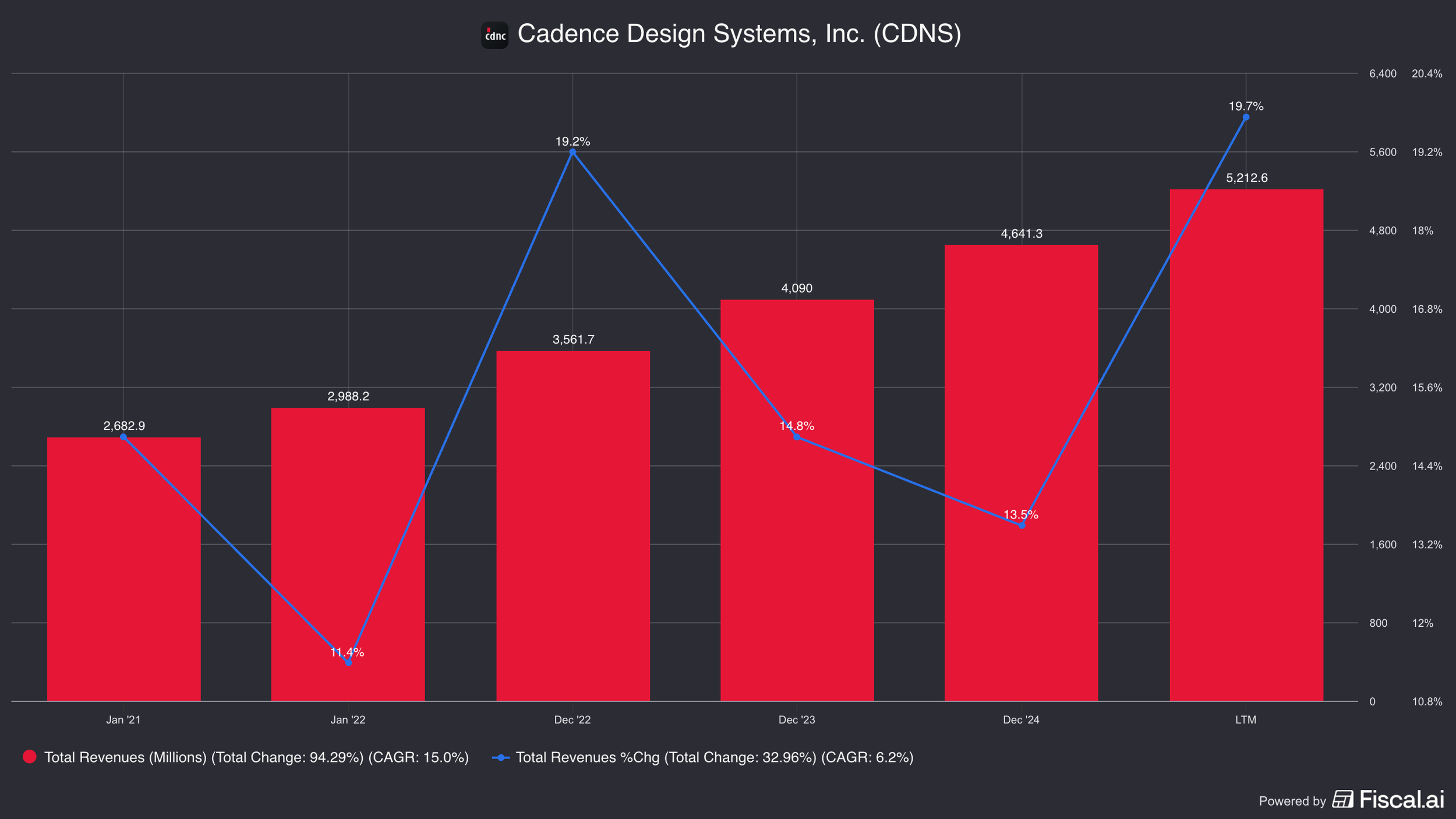
Cadence, at a $315 stock price, trades at a $87 billion enterprise value.
They currently generate $5.2bn in revenues.
If this grows 15% next year and they can increase margins a bit to 30%, they will trade at 60x NTM earnings.
Management has a goal of growing double digits long-term, but notes they have hit low teens the past 5 years.
If in 5 years, they can keep that up, they will have $10.5 billion in revenues.
They expect incremental margins of 50%. This implies margins will be just under 40% in 5 years.
This implies about $3.3bn in earnings in 2030.
Assuming they can still grow double digits, a 30x multiple could be fair.
Add back the cash they would generate over that time period of about $10 billion and we get a valuation of $110 billion.
This can also prove to be too optimistic if growth slows in 5 years from now.
However, if they continue to be instrumental to the semiconductor industry, it is possible investors place a premium multiple on it—even if it is hard to tie that multiple back to cash returns.
Ultimately, the assumptions an investor is comfortable with and the return they demand is on the judgement of the investor to decide…